
Self operated laboratory
 Home / Self Operated Laboratory
Laboratory EnvironmentQuality AssuranceTest EquipmentInspection items and costsAnalysis Case
Laboratory Environment
Laboratory Environment
According to the relevant standards of IPC J-STD-033B and MIL-D-3464E, the temperature and humidity of the laboratory environment have been strictly controlled; According to the JEDECJS-001-2017 standard, anti-static measures have been taken in all areas and processes from floor to shelf, from test bench to workbench, from unpacking to inspection, to ensure good anti-static environmental conditions.
Laboratory basis&standards: AS6081, IDEA-STD-1010-B, IPC-A-610D, etc

Quality Assurance

- ISO9001:2015
- ISO45001:2018
- ISO14001:2015
- ISO9001:2015
Test Equipment
- X-ray platform
- De-cap platform
- Metallographic microscope
- High magnification digital microscope
- Iv Curve Tracer
- Solderability testing tin furnace
-
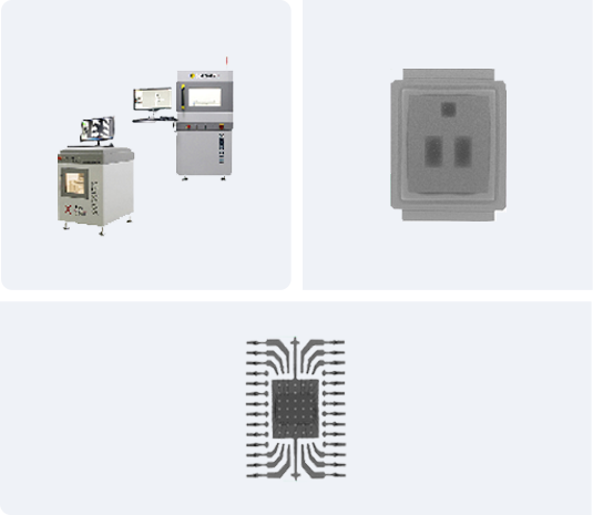
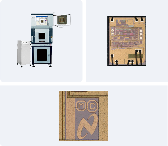
Overview of X-ray Platform
This device has a super large load testing platform that can tilt, observe, and detect photos from multiple angles, with an accuracy of up to 3um.
By using IQC incoming non-destructive testing and FA failure analysis, it is possible to compare standard samples and detect internal structures such as Wafer, Bonding, and Lead Frame. -
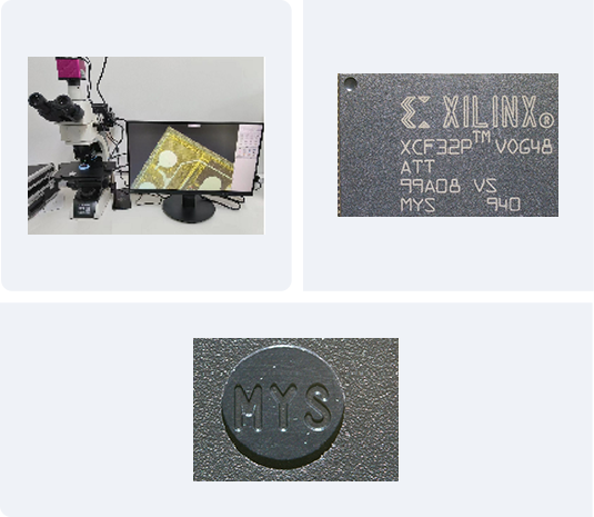
De cap platform
Multi stage adjustable laser setting, laser power 10w (adjustable), opening depth: 0.01mm -30mm, for rapid opening analysis of semiconductor products to observe the structure, logo, shape and version of the internal Wafer, bonding lead position and material, determine the authenticity of the material, and also observe Wafer damage abnormalities in failure analysis.
-
Metallographic microscope
Multiple light sources can be used to observe the material 360 degrees, with a magnification of up to 1000 times. This can be used for QC to inspect the entire appearance of the material, screen printing, and positioning holes to determine whether the material is refurbished.
-
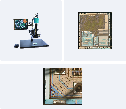
High magnification digital microscope
Used for device failure analysis, De-cap assisted observation, and can continuously autozoom from 100 to 1000 times. The lens can be tilted to 180 degrees to observe the internal structure and abnormalities of the Wafer. It can synthesize 3D models with super deep field and depth, and can remotely measure the size and height of various positions.
-
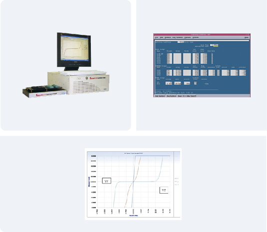
IV Curve Tracer
Used for semiconductor failure analysis, including open circuit/short circuit detection, eight curve tracing analysis, leakage detection, etc., can help customers quickly locate the failure location and find the cause of the failure.
-
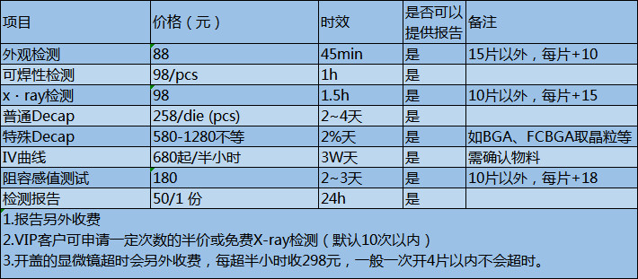
Soldering Pot
According to the JESD22-B102solderability standard, conduct solderability tests on various plug-in and SMT packaged devices.
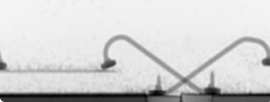
Inspection items and costs
Inspection items and costs
1.Visual Inspection
2.Solderability testing
3.X-RAY (Authenticity Detection and Failure Analysis)
4.DE-CAP (Authenticity Detection and Failure Analysis)
5.IV CURVE TRACER (Static electrical parameter analysis and failure analysis)
6.Resistance capacitance sensing parameter testing
Analysis Case

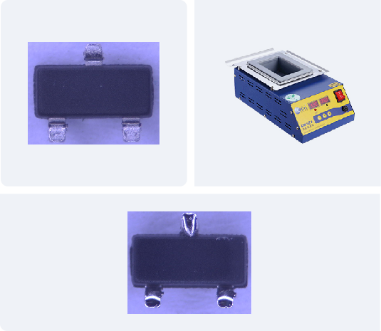
- 1.Appearance inspection: Refurbished materials
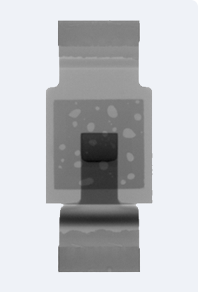
- 2.X-ray detection: Bonding bonding abnormality
- 3.X-ray detection: bubble detection
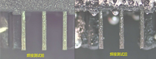
- 4.Solderability: Pin solder rejection, solderability NG
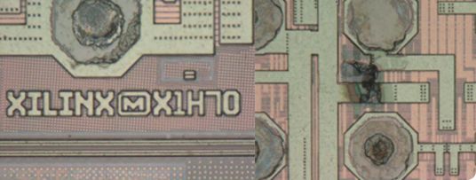
- 5.Decap: XILINX genuine, burnt out on machine


About UsProductsServiceQuality ControlNewsContact Us
West International Co., Ltd.
Address: RM 605, 6/F ,Hewlett Centre, 52-54 Hoi Yuen Road, Kwun Tong, Kowloon, Hong Kong.
Tel:+852 2130 7171
E-mail:info@westic.hk
Shanghai Woshi Electronics Co., Ltd
Address: 8th Floor, No. 25 Yixian Road, Yangpu District, Shanghai
Tel:+86(21) 6566 0166
E-mail:info@westic.hk
Copyright © 2023 Shanghai Woshi Electronics Co., Ltd
